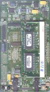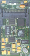

The fourth version of the SmartBadge builds on the lessons learned from the three earlier iterations which have been used in classes at KTH (Mobile Personal Communications module of the Telecommunications "finger" course during Spring 1997, 1998, 1999) and University of Wollongong (during Summer 1997). This version was designed in late 1999 by Dr. Mark T. Smith of HP Labs.
We encourage you to use the information from these pages, but would ask that you site as a source:
Mark T. Smith and Gerald Q. Maguire Jr., SmartBadge/BadgePad version 4,
HP Labs and Royal Institute of Technology (KTH),
http://web.ict.kth.se/~maguire/badge4.html, date of access yyyy-mm-dd.
This version is a 12 layer printed circuit board with ball grid array (BGA) mounted SA1110 processor and SA1111 companion chip.
The first badge of this version ran was operational (without the SA1111 chip) on Saturday 03-February 2001. It immediately ran the ARM Angel debugging environment. As of 03-July 2001 it is running Linux.
Scan of the partially assembled first badge Front (without a SO-DIMM card), Front (with 32MB SO-DIMM SDRAM in place), and Back.
Finished badge photos (from Mat Hans):
 |
 |
| Front | Back |
The basic system consists of a Intel StrongArm-1110 processor, StrongArm-1111 coprocessor, Flash, SRAM, sensors, some built-in communication links, a SO-DIMM socket, and both PCMCIA and Compact Flash interfaces.
Alternative for the future: Fenwall Electronics +1 508 478-6000, NTC surface mount end band thermistors - 100 Ohms to 1Megohm, 2-10%, $0.35 to $0.15 for quantities 5,00 to 100,000 [5% resistance tolerance at 25 degrees C]
PCMCIA (connector in place) and Compact Flash (must be connected via an adaptor to the board)
USB bus master support (Note: The USB connecter is attached to via small daughter card (USB dongle - described below), thus you can more flexibly position it in a case.)
USB Dongle (front) and (back).
The external USB dongle is connected to jack JP11 -- USB Host interface via a ribbon cable. Note carefully that the connectors are on opposite sides of the cable. The dongle itself is similar to a USB Self Powered Hub. The dongle has a TI SN75240 transient voltage suppressor to provide some ESD protection and reduce the risk of damage to the SA1111. There is also a TI TPS2014 Power Distribution Switch which enables or disables the badge to supply power to the USB connector. The dongle has a USB series A Receptacle which can be used to attach it to a hub or to peripherals.
Pin out on the USB dongle, with the USB connector at the top (as shown in the "front" picture above), pin 1 will be the lower lefthand corner of the lower row:
| USB dongle pin | PJ11 pinout | Name | Purpose |
|---|---|---|---|
| 1 | 10 | USBH_Wakeup SA1111 GPIO A3 | not connected at the dongle |
| 2 | 8 | 5V | input voltage to the TPS2014 |
| 3 | 6 | Ground | Ground |
| 4 | 4 | Ground | Ground |
| 5 | 2 | 3.3V | 3.3V supply |
| 6 | 1 | USBH_PWR_SEN | Connected to the Over Current (OC-) output of TPS2014 |
| 7 | 3 | USBH_PWR_CTL SA1111 GPIO A4 | Connected to the Enable (EN-) of TPS2014 enables/disable 5V power |
| 8 | 5 | USBH_M SA1111 USB_Minus | USB data signalling |
| 9 | 7 | USBH_P SA1111 USB_Plus | USB data signalling |
| 10 | 9 | USBH_Detach SA1111 GPIO A2 | not connected at the dongle |
Badge PJ11 pinout
| PJ11 pinout | Name | Purpose |
|---|---|---|
| 1 | USBH_PWR_SEN | Connected to the Over Current (OC-) output of TPS2014 |
| 2 | 3.3V | 3.3V supply |
| 3 | USBH_PWR_CTL SA1111 GPIO A4 | Connected to the Enable (EN-) of TPS2014 enables/disable 5V power |
| 4 | Ground | Ground |
| 5 | USBH_M SA1111 USB_Minus | USB data signalling |
| 6 | Ground | Ground |
| 7 | USBH_P SA1111 USB_Plus | USB data signalling |
| 8 | 5V | input voltage to the TPS2014 |
| 9 | USBH_Detach SA1111 GPIO A2 | not connected at the dongle |
| 10 | USBH_Wakeup SA1111 GPIO A3 | not connected at the dongle |
In order to use JTAG to program the FLASH memory you must hold down the reset switch (a small padded alligator clamp works well for this).
With an external battery pack which output 3V or less you can easily make a battery power supply for the badge. For example, a pair of rechargable 1.2 V cells in parallel attached in series to another parallel pair will work well.
In order to be able to use the RS-232 serial interfaces you need to modify the RS-232 serial board so that you can also run it from battery power. The easiest method of doing this is to remove the LM317LZ regulator (the smaller of the two regulators on the board) and solder a wire from pin 20 of the serial ribbon cable connector (the wider cable which runs to the badge) to the middle hole where the regulator was - this will connect the 3.3V which the badge now provides via pin 20 to the MAXIM part so that it can level shift the RS-232 signals.
Pinout of JP1 is:
| pin | name | purpose |
|---|---|---|
| 1 | UDC+ | serial port 0 of SA1110 - which can only used as a USB periperal |
| 2 | UDC- | |
| 3 | TXD_1 | serial port 1 |
| 4 | RXD_1 | serial port 1 |
| 5 | GND | ground |
| 6 | UART_HS1 | aka GP13 for GPIO |
| 7 | UART_HS2 | aka GP14 for GPIO |
| 8 | GND | ground |
| 9 | NC | Not Connected |
| 10 | NC | Not Connected |
| 11 | GND | ground |
| 12 | NC | Not Connected |
| 13 | NC | Not Connected |
| 14 | NC | Not Connected |
| 15 | NC | Not Connected |
| 16 | GND | ground |
| 17 | NC | Not Connected |
| 18 | TXD_3 | serial port 3 |
| 19 | RXD_3 | serial port 3 |
| 20 | 3.3V | 3.3V supplied by the badge |
JTAG 1149.1 connector which can be used for both debug and for in circuit programming of the FLASH memory. A second JTAG interface is used to program the CPLD (programmable logic).
A USB attached JTAG programmer (PDF) has been designed by Mark Smith. It is designed as a daughter card with a Texas Instruments TAP Master (74LVT8980A) which plugs into an ActiveWire-USB board (http://www.activewireinc.com/). This daughter card also provides an RS-232 interface (this could be used to provide the serial connection to either the ARM Angel tools or the Linux console).
Mark T. Smith's source code for controlling the TAP Master. This provides an example of how to program the Texas Instruments tap master controller. Note that this code was written to do JTAG transactions on a StrongARM SA1110 processor target; hence the relevant BSDL definitions are hard coded into it in the library source ARMPIT.C. The file "taputils_readme.pdf" within the ZIP file describes each of the other files.
Using the audio on the badge.
Don Loomis, "The TINI Specification and Developer's Guide",USB Addison-Wesley, 2001, ISBN 0-201-72218-6. Describes from a user's point of view how to use the TINI environment and board which Dallas Semiconductor has developed. This system utilizes a small Java system to make it rather easy for users to develop network attached sensors and adaptors. The book is quite readable and provides an excellent series of increasingly complex examples. This is the sort of book that should exist for every environment (perhaps this will serve as an incentive for someone to write such a book for the badge(s)).
Mat Hans's Badge4 page has links to where to get the bits for this version of the badge, a mailing list for uses of this version of the badge, etc.
Linux system development on an embedded device: Tinkering with PDAs for fun and profit by Anand K Santhanam and Vishal Kulkarni.
G.Q.Maguire Jr. (maguire@it.kth.se)