
Fig-11: Create PCB from schematic.
The PCB can be generated from the schematic using the Board button (Fig. 11).
Fig-11: Create PCB from schematic.
This brings up the pcb window.
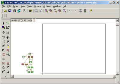
Fig-12: PCB layout window
Thin lines marks air wires, indicating the unconnected wires.
In the freeware version of Eagle components can only be placed in an area of 100x80 mm. This is indicated by a rectangle in the dimension layer. If trying to move components outside this area an error message will be generated.
In our PCB the size will be 30x40 mm. To make things easier we adjust the dimension to represent the size of the PCB. Adjust the size of the dimension using the move command (Edit->Move).
To make it easier to adjust to the correct size it is convenient to set the grid. To adjust the grid to 5mm, use the command View->Grid to bring up the grid menu (Fig. 13).
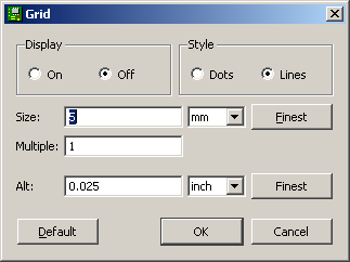
Fig-13: Set grid to 5 mm
The spacing between legs on circuits is usually in a grid of 100 mil, corresponding to 0.1 inch or 2.54 mm.
To make routing simple, adjust the grid to 50 mil (Fig. 14).
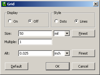
Fig-14: Set grid to 50 mil
When the PCB layout opens, all components from the schematic are automatically placed in the layout, but not in the correct location (Fig. 12).
Use the move function (Edit->Move) to move the components to a suitable location. This is the most critical part of the PCB layout, and the one that requires the most thought.
For moderate or large size PCB design it is often recommended to do "floor planning", where components with many connections are located close to each other. Often several iterations are required to achieve a good layout.
Tip For moderate or small layouts the floor planning can be done using pen and paper.
After moving the components the air wires will be incorrect. By pressing the ratnest button (Fig. 15) the wires are recalculated to indicated the shortest distance.

Fig-15: Ratsnest button
Since we are using a single sided PCB all surface mounted components must be placed on the solder side (bottom) of the PCB. Traces in the bottom layer is indicated by blue colour.
In order to move the capacitors and resistors to the back layer, use the mirror component function (Edit->Mirror)
When the PCB size is adjusted and components are moved to the correct layer the PCB should look like figure 16.
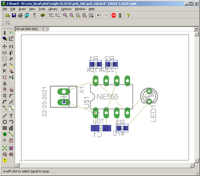
Fig-16: Components moved to correct location
The next step is to route the wires. Do this using the Edit->Route function.
NOTE Always use the Route function in order to keep the schematic and layout synchronised. If placing wires using the Wire function connectivity between schematic and layout is lost.
When selecting the routing function the status bar at the top of the window is activated (Fig. 17).

Fig-17: Select routing layer and wire width
Select the bottom layer to route the PCB, and set the wire width to 24 mil.
When routing the software helps you to keep the wires in 45 degree angles. You may change the way the wire is routed by pressing the right mouse button.
Deleting wires using the ripup function (Edit->Ripup). Don't use the Delete function since this will destroy the connectivity between schematic and layout.
When routing multi-layer PCB a via is automatically added when changing layer.
The final layout should look something like figure 18.
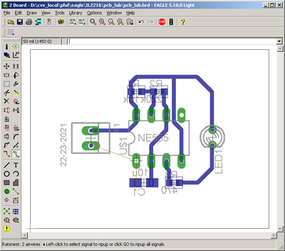
Fig-18: Routed PCB (except GND)
Note that one wire is not connected. This wire we will connect using ground plane.
High frequency designs often use a ground planes to achieve good grounding.
Add the ground plane by drawing a polygon (Draw->Polygon). Place the polygon around the corners of the PCB (Fig. 19).
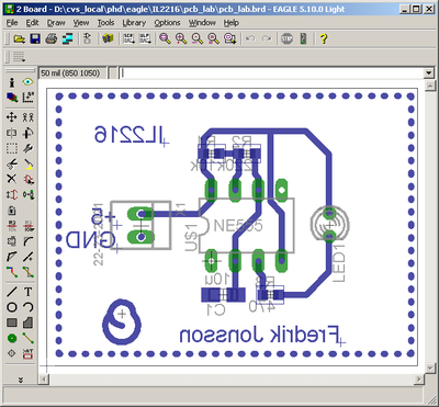
Fig-19: Add polygon
Since the ground plane have no symbol in the schematic it is not connected to the ground net by default. In order to connect the ground plane to the correct net we must manually specify the net. Use the Edit->Name function, select the polygon and specify the net to GND (Fig. 20).
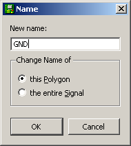
Fig-20: Connect polygon to GND net
When pressing ratsnest the ground plane is calculated. Pins connected to GND are connected to the plane using thermal connections, while connections to other nets are avoided using a specified clearance.
To adjust the clearance, use the Edit->Change and select Isolate function to set the clearance. Adjust the clearance to 12 mil.
Finally, add text or other useful information to identify the PCB. When making PCB using a factory text and other information information is added using graphical screen print. In our lab we don't have this option, and text are instead added directly into the copper.
Example of the final PCB is illustrated in figure 21.
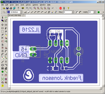
Fig-21: Final PCB layout
Note that since we are using the back side of the PCB the text looks mirrored on the screen.