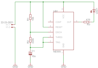
Fig-1: Simple LED flasher using 555 timer circuit
This tutorial is a brief introduction to PCB design using the EAGLE CAD tool. Eagle is a simple Computer Aided Design (CAD) that can be freely downloaded and used for non-commercial applications. The goal of the lab is to create a simple Printed Circuit Board (PCB). As an example circuit we use a timer (Fig. 1) to flash a LED.
Fig-1: Simple LED flasher using 555 timer circuit
The tutorial is in no way a complete guide to all functions available in EAGLE. Please refer to the EAGLE documentation, or tutorials available on the Internet for more information.
Eagle can be freely downloaded from the Cadsoft website.
http://www.cadsoft.de/freeware.htm
Download and install Eagle from the tool website:
Start the tool in Freeware mode.
When you start Eagle the control panel opens (Fig. 2).
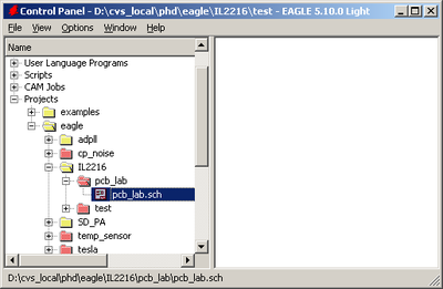
Fig-2: Eagle control panel
Using the control panel you can open and manage libraries and designs.
Libraries contains predefined components and footprints from different manufactures. All basic components such as resistors, standard IC circuits and connectors are available in the library. For special components not available from default you may need to create your own library.
Design Rules The design rules contain rules for dimension and spacing when manufacturing PCB boards.
User Language Programs and Scripts contains various scripts. Eagle have a built in programming language to perform special tasks.
CAM Jobs contain various method for exporting data to Computer Aided Manufacturing (CAM) machines. These jobs are required when sending PCB for manufacturing.
Projects contain examples and your project data.
By default all projects are stored in the installation directory. If you prefer a different location for your designs you can configure the directly location using the Options->Directories menu.

Fig-3: Directory setup
In the example Fig. 3 the projects directory is configured to also include the two directories:
 $EAGLEDIR\projects\examples
 d:\cvs_local\phd\eagle
$EAGLEDIR is the path to the Eagle install directory.
Create a project library using the menu File->New->Project
Select this project and create a schematic using the menu File->New->Schematic
When creating the schematic an empty schematic window opens (Fig. 4)
Fig-4: Directory setup
The new schematic is still untitled. Use the Save as function to save the schematic using the name you want.
Select the Edit->Add menu to add components, or use the button (Fig. 5).

Fig-5: Add component
This brings up the library browser (Fig. 6).
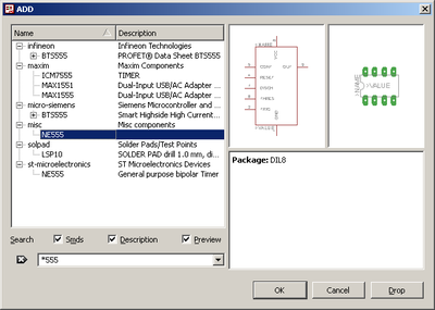
Fig-6: Component library browser. Search for components using the filter option. To view all libraries, clear the search field.
Select the 555 timing circuit from the
misc/NE555 library
You can easily find components using the search field.
Various resistors and capacitors can be found in the rlc library. Use 0603 resistor footprint using the R-EU_ footprint for European symbols.
rlc/R-EU_/R0603
and capacitor using the 3216 package:
rlc/CPOL-EUA/3216-18W
Place the components in the schematic. When placing the components you can rotate the symbol using the right mouse button.
To mirror the component, place the component in the schematic, select the mirror function (Fig. 7) and click the component you want to mirror.

Fig-7: Mirror component
Set value of the component using the Value function (Fig. 8). By default the name of the component is assigned automatically (R1, R2 etc.). If you want you can also specify the name of the component. Remember that two components can not have the same name, this will create an error message.

Fig-8: Set component value
For the GND connections use
supply1/GND
This generates a global net named GND. All components connected to this net are connected even when there are no visible wire in the schematic.
Finally add a connector to be able to connect the power cable. Use for example the
con-molex/22-23-2021
two pin connector.
If you want to change the package at a later stage you can do this using the Edit->Change menu and select the Package option.
You can move components using the Edit->Move menu, and selecting the component you want to move.
Use the side scrollbars or the mouse wheel and button to pan and zoom in the window.
A convenient way to move around the window is to zoom out using the wheel, and then zoom in on the area you are interested in.
To fit the whole schematic in the window, press the zoom-fit button (Fig. 9).

Fig-9: Fit schematic in window
When you have placed the components in the schematic you need to connect them using wires. Add wires using the Draw->Wire menu, or by using the add wire button (Fig. 10).

Fig-10: Add wire
Be careful when adding wires, they need to connect to the very pin of the components.
Add the junctions to connect the different wires using Draw->Junction menu.
The final schematic should look like Fig. 1.
Tip: one method to check if all wires are correctly connected to the component is to move the component. If the wires follows when moving they are correctly connected. If not moving they will be connected is the component is placed in the original position.
The PCB can be generated from the schematic using the Board button (Fig. 11).

Fig-11: Create PCB from schematic.
This brings up the pcb window.
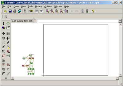
Fig-12: PCB layout window
Thin lines marks air wires, indicating the unconnected wires.
In the freeware version of Eagle components can only be placed in an area of 100x80 mm. This is indicated by a rectangle in the dimension layer. If trying to move components outside this area an error message will be generated.
In our PCB the size will be 30x40 mm. To make things easier we adjust the dimension to represent the size of the PCB. Adjust the size of the dimension using the move command (Edit->Move).
To make it easier to adjust to the correct size it is convenient to set the grid. To adjust the grid to 5mm, use the command View->Grid to bring up the grid menu (Fig. 13).
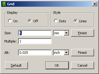
Fig-13: Set grid to 5 mm
The spacing between legs on circuits is usually in a grid of 100 mil, corresponding to 0.1 inch or 2.54 mm.
To make routing simple, adjust the grid to 50 mil (Fig. 14).
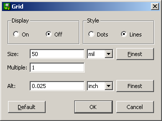
Fig-14: Set grid to 50 mil
When the PCB layout opens, all components from the schematic are automatically placed in the layout, but not in the correct location (Fig. 12).
Use the move function (Edit->Move) to move the components to a suitable location. This is the most critical part of the PCB layout, and the one that requires the most thought.
For moderate or large size PCB design it is often recommended to do "floor planning", where components with many connections are located close to each other. Often several iterations are required to achieve a good layout.
Tip For moderate or small layouts the floor planning can be done using pen and paper.
After moving the components the air wires will be incorrect. By pressing the ratnest button (Fig. 15) the wires are recalculated to indicated the shortest distance.

Fig-15: Ratsnest button
Since we are using a single sided PCB all surface mounted components must be placed on the solder side (bottom) of the PCB. Traces in the bottom layer is indicated by blue colour.
In order to move the capacitors and resistors to the back layer, use the mirror component function (Edit->Mirror)
When the PCB size is adjusted and components are moved to the correct layer the PCB should look like figure 16.
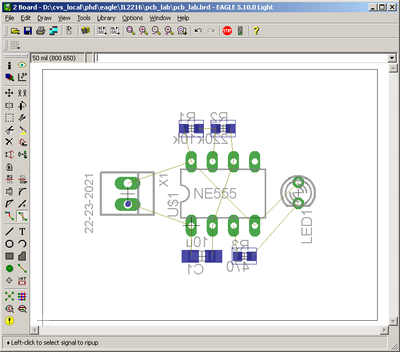
Fig-16: Components moved to correct location
The next step is to route the wires. Do this using the Edit->Route function.
NOTE Always use the Route function in order to keep the schematic and layout synchronised. If placing wires using the Wire function connectivity between schematic and layout is lost.
When selecting the routing function the status bar at the top of the window is activated (Fig. 17).

Fig-17: Select routing layer and wire width
Select the bottom layer to route the PCB, and set the wire width to 24 mil.
When routing the software helps you to keep the wires in 45 degree angles. You may change the way the wire is routed by pressing the right mouse button.
Deleting wires using the ripup function (Edit->Ripup). Don't use the Delete function since this will destroy the connectivity between schematic and layout.
When routing multi-layer PCB a via is automatically added when changing layer.
The final layout should look something like figure 18.
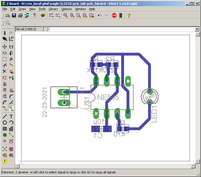
Fig-18: Routed PCB (except GND)
Note that one wire is not connected. This wire we will connect using ground plane.
High frequency designs often use a ground planes to achieve good grounding.
Add the ground plane by drawing a polygon (Draw->Polygon). Place the polygon around the corners of the PCB (Fig. 19).
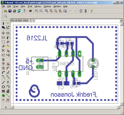
Fig-19: Add polygon
Since the ground plane have no symbol in the schematic it is not connected to the ground net by default. In order to connect the ground plane to the correct net we must manually specify the net. Use the Edit->Name function, select the polygon and specify the net to GND (Fig. 20).
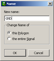
Fig-20: Connect polygon to GND net
When pressing ratsnest the ground plane is calculated. Pins connected to GND are connected to the plane using thermal connections, while connections to other nets are avoided using a specified clearance.
To adjust the clearance, use the Edit->Change and select Isolate function to set the clearance. Adjust the clearance to 12 mil.
Finally, add text or other useful information to identify the PCB. When making PCB using a factory text and other information information is added using graphical screen print. In our lab we don't have this option, and text are instead added directly into the copper.
Example of the final PCB is illustrated in figure 21.
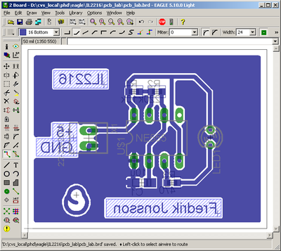
Fig-21: Final PCB layout
Note that since we are using the back side of the PCB the text looks mirrored on the screen.
Finally run checks that all connections are correct and that the PCB do not violate any design rules.
Ratsnest When pressing ratsnest, check that the message at the bottom of the window is Nothing to do. If there are still unconnected wires the number of airwires will be indicated. Make sure there are no unconnected wires.
ERC Run the Electrical Rule Check to check that two output ports are short circuited etc. Warnings that LED have no components have no value can be ignored.
DRC Runt the Design Rule Check to check clearance etc. Warning of non vector fonts can be ignored.
When sending PCB for manufacturing formats like Gerber 274x and Excellon drill files are used. Please refer to the Eagle documentation how to use the CAM processor to export to these formats.
In this exercise we use direct photographic transfer and print the layout using scale 2:1.
In order to print only the copper layer we need to setup correct visual layers. Set the visual layer using View->Display/hide layers to bring up the visual layers menu. Select layer 16, 17 and 18 visible, and keep all other layers turned off. (Fig. 22).
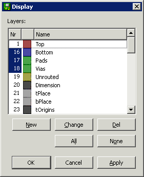
Fig-22: Layer setup to print bottom layer
To print the layout, use File->Print menu option (Fig. 23). Select the correct Scale factor and select Solid and Black to make the layout print in black colour rather than gray scale.
In order to print the back side correctly, also select the Mirror option.
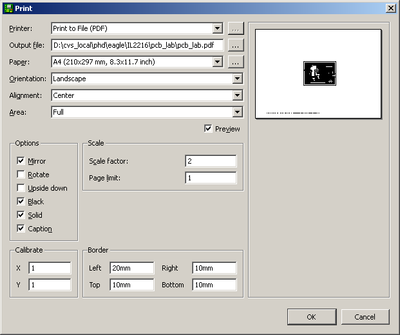
Fig-23: Print setup. Set the scale, check black, solid and correct mirror option
The final printout should be correctly mirrored in solid black color (Fig. 24).
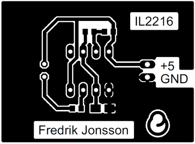
Fig-24: Printed layout. Check that the scale is 200%.
Print the layout and bring to the lab.
After printing the layout, restore the visible layers to the default values according to figure 25. If the layers are not restored it may not be possible to move components etc. in the layout.
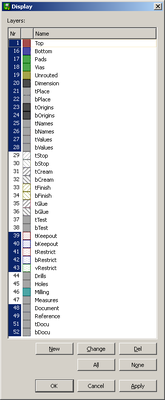
Fig-25: Restore default layers
Please check that all the following are done before manufacturing the PCB:
Electrical connections Check that all connections and all components are correctly connected in the layout and schematic.
Layer Check that all resistors and capacitors are placed on the correct layer. Remember that we are using a single layer PCB in this exercise, so all capacitors and resistors must be placed on the back side.
Size Print the PCB in scale 1:1 and measure using a ruler that the size is correct. If you have components available it is also a good idea to place the resistors and other components on the paper to see that the components will fit physically and that the footprints are correct.
Run checks Run the ERC and DRC check.
Print When everything is OK, print the layout in black and white and bring to the PCB lab.